Reducing Signal Integrity Issues on High-Frequency IC Boards
For engineers working with RF modules, Wi-Fi 6/7, or other jittery (high-frequency) integrated circuits, signal integrity is critical for maximizing products to their greatest potential. The highest quality components can fail if the printed circuit board layout does not take into account the basics of SI. This in-depth technical guide identifies and discusses the most important design steps (e.g., Impedance Matching, Differential Pair Routing, Parysitic Control) the most common problems related to SI. This document also covers important SI analysis methods and pre-layout analysis techniques that will guarantee the best possible results in your high-speed PCB designs for RF/Wi-Fi applications.

Matching High Frequency Impedance, 50Ω vs 100Ω
There's a big concern with impedance discontinuity when designing at higher frequencies because it can cause problems with signal reflection, attenuation and/or timing. Most of the time, when designing Printed Circuit Boards (PCBs) at these high frequencies, two sets of standard characteristic impedances are used and the impedance matching is dedicated to the type of signal being created.
50Ω for RF & Single-Ended Signals
Most RF modules (Bluetooth, Zigbee, etc.), Wi-Fi transceivers and the majority of single-ended high-speed signals utilize a characteristic impedance of 50Ω. The way to ensure you keep this number 50Ω would be:
Control the Width of the traces on your PCB and the thickness of the PCB substrate. For the standard FR-4 material (dielectric constant ~ 4.4), a microstrip trace with 50Ω characteristic impedance would be approximately 0.8mm in width on a PCB with a standard thickness of 1.6mm (you may need to make adjustments based on your specific substrate data sheet).
Avoid creating any sudden changes in width on your traces or creating right-handed bends in the traces. Both conditions create an impedance discontinuity. Instead, use 45° bends or curves in your trace to maintain a consistent characteristic impedance.
Keep your traces a minimum of three times their width from the edges of your PCB to avoid the potential of impedance drift from the edge effect.
Differential Pair - 100Ω
Differential pairs (or Balanced Signals) in Wi-Fi 6/7 Data Lanes, USB3.0+, and Ethernet all require Differential Impedance of 100Ω.
When designing PCB tracks for Differential Pairs, ensure that you:
Have tracks that are the same length and the same distance apart from each other. Distance between two tracks in a differential pair will be 0.5X to 1X the width of the track (i.e., If the track width is 0.4mm then the gap between the two tracks of the differential pair should be 0.4mm or 0.2mm).
Use your PCB Design Software (for example, Altium/KiCad) to calculate Differential Impedance, taking into consideration the Dielectric Constant of your Substrate and the Stackup of the Layers within your Board. This tool will ensure that you maintain controlled impedance routing and avoid Impedance Discontinuities.
Wireless Technologies using Differential Pair Routing

Gain greater immunity to noise and crosstalk during high-speed transmissions (up to 30 Gbps with Wi-Fi 6/7) through improved RF signal robustness by ensuring the pairing of differential signals on the PCB maintains a perfect balance through common mode interference cancelation. The following rules provide guidance on how best to route differential pairs:
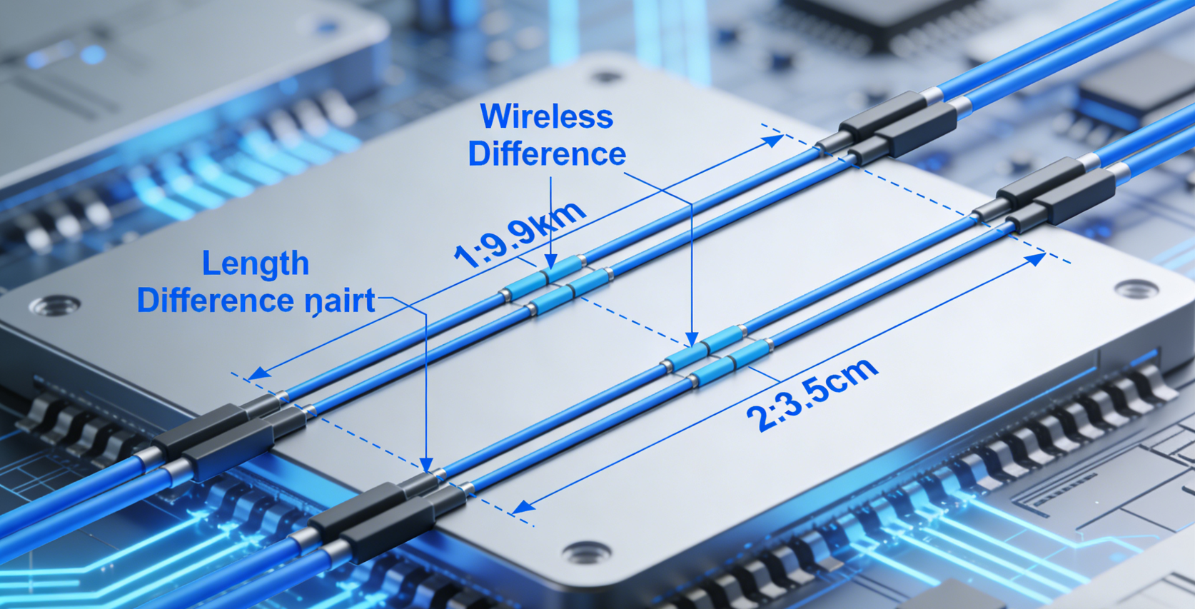
Ensure that the lengths of the individual pair traces are equal and parallel to one another.
When one trace is shorter than the other, and hence there is a degree of skew (i.e. the signal is delayed) between them. The maximum allowable length difference for Wi-Fi 7 is 2 mm, while for Wi-Fi 6 it is 5 mm. If a difference in length exists, then utilize serpentine tracing (gentle curves) to achieve equal lengths; do NOT use extremely tight loops that add parasitic inductance and delay signals propagating.
Keep differential pairs from being close together.
To minimize crosstalk between pairs, separate their routing by a distance of at least 3 times their individual spacing; e.g., a pair that has a spacing of 0.4 mm must be routed with at least a 1.2 mm gap separating them. Under no circumstances should other signals be routed between a differential pair of transmission lines. Maintaining the minimum separation distance will minimize the amount of broadside coupling, mutual capacitance, and maximize the differential immunity to crosstalk.
Minimize Via Usage
Vias add parasitic capacitance and inductance, which can negatively impact signal integrity. If you must use vias for a differential pair, place them side-by-side (not staggered) and keep the number equal for both traces. Use blind/buried vias (instead of through-vias) for HDI boards to reduce impedance changes and maintain signal integrity.
Control of Parasitic Parameters
Traces, vias, and component layout can contribute parasitic inductance (L) and capacitance (C) which will degrade the quality of high-frequency signals. This section is intended to provide guidelines on mitigating parasitic inductance and capacitance.
Reducing Parasitic Effects in Traces
The shorter you keep a high-frequency trace, the less inductance and attenuation there will be. Long traces have more length than they can carry, and they will create additional loop inductance. You should use as few vias as possible in your designs. In fact, you should avoid using vias altogether when possible. If using vias is necessary, you should use a wide ground fill located directly below the signal trace (this is known as a micro-strip design). By using a wide ground plane like this you will also lower your loop inductance, control inductive coupling between traces, as well as reduce mutual inductance between traces. All of these reasons help to control electromagnetic interference (EMI) and thus improve your signal integrity.
Component Placement
When designing with RF/Wi-Fi components it is very important that you place decoupling capacitors (both 0.1uF and 10uF) as close to the IC power pins as possible. Also keep in mind that you should always try to keep RF/Wi-Fi IC's as far away from large power supply and high-current components as you can. You should never allow any component to be within 10mm of another component without an intervening ground or power plane. Proper placement of components and creating proper power and ground paths is important to designing a durable power distribution network for high-speed digital designs and reducing capacitive coupling between components.
Substrate Selection
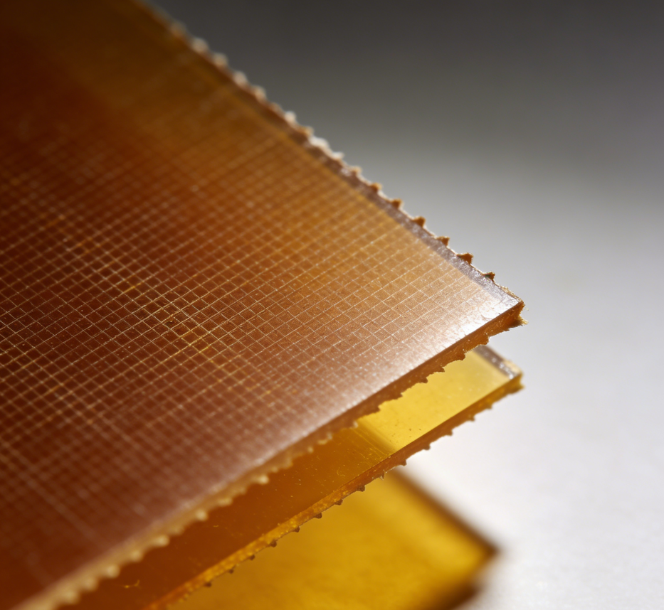
A substrate material that is designed for use with Wi-Fi 7 or high-power RF components (>10 GHz) should be made from a high-performance substrate. High-performance substrates have much lower dielectric loss (Df) compared to the standard FR-4 material and will maintain their characteristic impedance over a wide frequency range. This means they will minimize the amount of attenuation and distortion created by the nearby electromagnetic fields.

Solutions for Fixing Crosstalk and Signal Loss
Crosstalk and signal loss (or "attenuation") are considered to be the two main issues affecting the integrity of the signal when designing circuits that operate at high rates of frequency. The following are some potential solutions for resolving crosstalk and attenuation issues:
Reducing Crosstalk
1. Use Grounded Guards: Insert a grounded trace between high-speed signals and all other traces on the same layer. Place the guard 0.5 mm away from each trace to minimize capacitance between traces. This solution works well for minimizing NEXT and FEXT.
2. Optimize the Layer Stackup: Route any signals that operate at or above 1 GHz on an inner layer (using a stripline configuration) and place ground planes on both the top and bottom sides of the signals. Ground shielded signals are less susceptible to electromagnetic coupling than signals routed in a micromultilayer configuration on an outer layer.
Reducing Signal Attenuation
Do not Use High Loss Materials: If you are designing a circuit to operate at frequencies higher than 5 GHz, it is best to avoid using FR-4. It has a very high Df (dielectric factor), which creates excessive attenuation and distortion. Using low-loss substrates will help you maintain the integrity of your signals.
Control Trace Impedance: As mentioned previously, the impedance of your traces must be matched to minimize reflection and, ultimately, to minimize the amount of attenuation. You should be using controlled impedance routings to maintain the same characteristic impedance throughout the signal path. If you have a change in the impedance of the trace, the reflected signal will be distorted.

Basic Troubleshooting Methods
If you observe an occurrence of signal reflection, examine your circuitry for impedance discontinuities by performing an s-parameter analysis with the use of a network analyser. Another common cause of an impedance jump is a sudden change in the trace geometry of the PCB. An efficient way to reduce the likelihood of discontinuities in impedance is to modify your trace width or add impedance matching stubs.
Should you have a high level of crosstalk between your signal traces, consider providing more spacing between the traces; placing ground guards between traces; or routing your signal wires to inner layers of the PCB. The use of crosstalk analysis tools can help you identify sources of mutual capacitance and electromagnetic coupling that cause your crosstalk.
In situations when you have Wi-Fi or RF equipment with limited signal range, inspect for an excessive number of vias or long lengths of trace/plane proximity to the antenna; also make certain that the feed line connecting the antenna has a 50-ohm characteristic impedance and does not have a connection with other PCB devices or traces. Doing a good job of following signal return paths will help to retain signal integrity and reduce distortion.
If you examine the basics of signal integrity and apply the correct metrics for the analysis of signal integrity, then your high-frequency integrated circuit (IC) printed circuit boards (PCBs) will operate as designed in a practical environment. The success of high-speed PCB designs is best achieved through a coordinated effort using prelayout research, electromagnetic simulations, and postlayout evaluations to evaluate and correct for potential signal integrity problems related to impedance mismatches. We welcome any request to review custom layouts or provide recommendations regarding substrates for RF/WiFi designs.


